
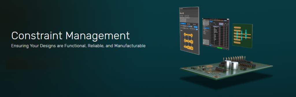
Discover how to ensure your designs are functional, reliable, and manufacturable with our five-part Constraint Management Design Guide.
- Part 1
This Constraint Management guide will help you understand the importance of constraints and learn how to create and apply them to optimize the signal integrity, reliability, and manufacturability of your PCB designs. - Part 2
Explore this guide to learn how to set standard constraints and rules that form the backbone of PCB design. These constraints range from physical and spacing rules to manufacturing, helping ensure that you’re designing a reliable and compliant PCB layout. - Part 3
This guide explores advanced PCB design constraints, focusing on high-speed and electrical design rules such as net scheduling, impedance control, and differential pairs. These constraints are crucial for maintaining signal integrity and timing precision in high-speed interfaces like USB, DDR, PCIe, and RF circuits, ensuring performance and reliability. - Part 4
This part of the guide covers optimization techniques in PCB constraint management, focusing on ECSets, schematic-to-PCB constraints, and the modular approach. These tools help streamline workflows, ensure consistent constraint application, and maximize design efficiency for better results. - Part 5
This final part of this guide uses a practical project example to demonstrate the application of learned constraint management concepts. Through a practical case study, it reinforces key insights and helps highlight the effectiveness of proper constraint management during the PCB design process, ensuring that readers can tackle design challenges with confidence.