

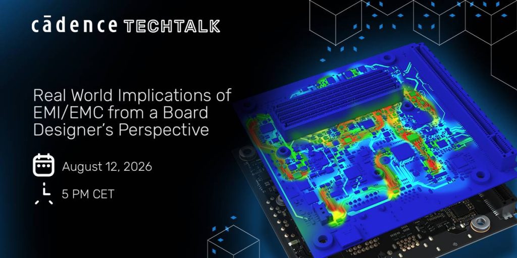
Real World Implications of EMI/EMC from a Board Designer’s Perspective
Reducing EMI/EMC issues starts long before testing, and the decisions made during PCB layout can have a significant impact on whether a design passes the first time.
Join us for this webinar where Senior PCB Designers Matthew Leary and Lauren Waslick, along with Senior Electrical Engineer Myev Bodenhofer from Newgrange Design, draw on decades of combined design experience to share lessons from real PCB projects and the practices needed to minimize EMI/EMC risks early in the design process.
Here’s what will be covered:
- Practical EMI/EMC design best practices based on real-world PCB projects
- How to develop an EMI/EMC-focused design mindset from the start of a project
- Layer stackup strategies that support better electromagnetic performance
- Why ground planes are critical for reducing EMI issues
- When and where to use stitching vias to improve board performance
- Actionable techniques to reduce design risk and improve the likelihood of first-pass success
Reserve your spot today and get your questions answered during the live Q&A
Unable to attend live? Register anyway and we will send you the recording so you can watch it at your convenience.
Clicking the link will redirect you to Cadence’s registration page

